Digital Logic Concepts Quiz
Digital Logic
Unit 1: Introduction
1.1 Digital Signals and Waveforms
Definition
A digital signal is a discrete signal that represents data in binary form (0s and 1s). Unlike analog signals, digital signals do not vary continuously but have specific discrete levels.
Characteristics of Digital Signals
- Binary Representation: Two distinct voltage levels:
- High voltage = 1
- Low voltage = 0
- Discrete Time Intervals: The signal is sampled at fixed intervals.
- Noise Resistance: Less affected by noise compared to analog signals.
- Waveforms: Typically represented as square waves.
Waveform Representation
A digital waveform alternates between high and low states.
| Key Parameters | Description |
|---|---|
| Amplitude | Voltage levels (high and low). |
| Time Period (T) | Duration of one complete cycle. |
| Frequency (f) | , the number of cycles per second. |
| Duty Cycle | . |
Diagram:
  High ----
          |        _______
          |       |       |
  Low ----|_______|       |_______
             Time ->
1.2 Digital Logic and Operation
Definition
Digital logic is the foundation of digital systems. It uses logic gates (AND, OR, NOT, etc.) to process binary data (0s and 1s).
Key Components
- Logic Gates: Perform basic operations on binary data:
- AND, OR, NOT
- NAND, NOR, XOR, XNOR (derived gates).
- Boolean Algebra: A mathematical framework to simplify logic expressions.
- Combinational Circuits: Circuits where the output depends only on the current input (e.g., Adders, Multiplexers).
- Sequential Circuits: Circuits with memory elements where the output depends on the current input and past states (e.g., Flip-Flops, Counters).
Applications of Digital Logic
- Arithmetic operations.
- Control systems.
- Signal processing.
1.3 Digital Computers and Integrated Circuits (IC)
Digital Computers
A digital computer operates using digital signals and processes binary data. It consists of the following key components:
- Input Unit: Converts user data into digital signals.
- Central Processing Unit (CPU): Processes data using logic circuits.
- Memory Unit: Stores instructions and data.
- Output Unit: Converts digital data into human-readable form.
Integrated Circuits (ICs)
An Integrated Circuit (IC) is a compact electronic circuit made by embedding multiple components (transistors, resistors, etc.) into a single chip.
Types of ICs
- Small Scale Integration (SSI): Few gates per chip.
- Medium Scale Integration (MSI): Hundreds of gates per chip.
- Large Scale Integration (LSI): Thousands of gates per chip (used in CPUs).
- Very Large Scale Integration (VLSI): Millions of gates per chip (used in advanced processors).
Applications
- Computers.
- Telecommunication systems.
- Control systems in electronics.
1.4 Clock Waveform
Definition
A clock waveform is a periodic signal used to synchronize operations in digital circuits. The clock ensures that all components operate in coordination.
Characteristics
- Periodicity: Alternates between high (1) and low (0) at regular intervals.
- Frequency: Determines the speed of operation of the circuit ().
- Duty Cycle: Fraction of time the clock remains high in one cycle.
Diagram of Clock Waveform
  High ----
          |        _______         _______
          |       |       |       |       |
  Low ----|_______|       |_______|       |_______
             T1    T2        T3      T4    Time ->
Applications
- Timing control in processors and memory.
- Synchronization in sequential circuits.
- Frequency division in counters.
Unit2: Number System
1.1 Introduction to Number Systems
A number system defines a set of values to represent quantities. It is a mathematical notation for representing numbers of a given set. Digital computers operate on different number systems, with the most common ones being:
- Decimal (Base 10)
- Binary (Base 2)
- Octal (Base 8)
- Hexadecimal (Base 16)
Each number system is characterized by its base (radix), which is the total number of unique digits, including zero, used to represent numbers.
1.2 Types of Number Systems
1.2.1 Decimal Number System
- Base: 10
- Digits: 0, 1, 2, 3, 4, 5, 6, 7, 8, 9
- Positional Value: Each digit's position represents a power of 10.
- Example: .
1.2.2 Binary Number System
- Base: 2
- Digits: 0, 1
- Used in: Digital electronics and computers for logic representation.
- Positional Value: Each digit represents a power of 2.
- Example: .
Diagram: Binary Representation
1.2.3 Octal Number System
- Base: 8
- Digits: 0, 1, 2, 3, 4, 5, 6, 7
- Positional Value: Each digit represents a power of 8.
- Example: .
1.2.4 Hexadecimal Number System
- Base: 16
- Digits: 0, 1, 2, 3, 4, 5, 6, 7, 8, 9, A (10), B (11), C (12), D (13), E (14), F (15)
- Positional Value: Each digit represents a power of 16.
- Example: .
1.3 Conversion Between Number Systems
To convert numbers between systems, different techniques are used:
1.3.1 Binary to Decimal Conversion
Sum the positional values:
Example: .
1.3.2 Decimal to Binary Conversion
Repeatedly divide the number by 2 and record remainders.
Example: Convert :
- remainder
- remainder
- remainder
- remainder
- remainder
Binary: .
Diagram: Decimal to Binary Conversion
Unit 3: Combinational Logic Design
2.1 Introduction to Boolean Algebra
Boolean algebra, developed by George Boole, is the foundation of digital logic. It involves mathematical operations on binary values (0 and 1), which represent False and True, respectively.
2.2 Basic Boolean Operations
2.2.1 AND Operation
- Symbol: or
- Rule: if and only if and .
- Truth Table:
| A | B | | |---|---|-------------| | 0 | 0 | 0 | | 0 | 1 | 0 | | 1 | 0 | 0 | | 1 | 1 | 1 |
2.2.2 OR Operation
- Symbol: or
- Rule: if either or .
- Truth Table:
| A | B | | |---|---|-------------| | 0 | 0 | 0 | | 0 | 1 | 1 | | 1 | 0 | 1 | | 1 | 1 | 1 |
2.2.3 NOT Operation
- Symbol: or
- Rule: if , and if .
- Truth Table:
| A | | |---|-------------| | 0 | 1 | | 1 | 0 |
2.3 Laws of Boolean Algebra
2.3.1 Commutative Laws
2.3.2 Associative Laws
2.3.3 Distributive Laws
2.4 Simplification Using Boolean Laws
Simplification of Boolean expressions reduces circuit complexity.
Example
Simplify :
- Apply Distributive Law:
- Simplify using :
- Apply Absorption Law: .
2.5 De Morgan’s Theorems
De Morgan’s Theorems are crucial for simplifying complemented expressions:
1st Theorem:
2nd Theorem:
Proof for 1st Theorem
| A | B | |||||
|---|---|---|---|---|---|---|
| 0 | 0 | 0 | 1 | 1 | 1 | 1 |
| 0 | 1 | 0 | 1 | 0 | 1 | 1 |
| 1 | 0 | 0 | 0 | 1 | 1 | 1 |
| 1 | 1 | 1 | 0 | 0 | 0 | 0 |
Diagram: Basic Logic Gate Symbols
AND Gate
   A ----| & |---- Output (A · B)
   B ----|
OR Gate
   A ----|≥1|---- Output (A + B)
   B ----|
NOT Gate
A ----|>o---- Output (¬A)
Unit 4: Counters and Registors
3.1 Introduction to Logic Gates
Logic gates are the building blocks of digital circuits. They perform basic logical functions and are implemented using diodes, transistors, or integrated circuits. Each gate corresponds to a Boolean function and has a specific truth table.
3.2 Types of Basic Logic Gates
3.2.1 AND Gate
- Symbol:
- Function: Outputs 1 if all inputs are 1.
- Truth Table:
| Input A | Input B | Output | |---------|---------|-----------------------| | 0 | 0 | 0 | | 0 | 1 | 0 | | 1 | 0 | 0 | | 1 | 1 | 1 |
Diagram:
   A ----| & |---- Output
   B ----|
3.2.2 OR Gate
- Symbol:
- Function: Outputs 1 if at least one input is 1.
- Truth Table:
| Input A | Input B | Output | |---------|---------|-------------------| | 0 | 0 | 0 | | 0 | 1 | 1 | | 1 | 0 | 1 | | 1 | 1 | 1 |
Diagram:
   A ----|≥1|---- Output
   B ----|
3.2.3 NOT Gate
- Symbol:
- Function: Inverts the input.
- Truth Table:
| Input A | Output | |---------|--------------------------| | 0 | 1 | | 1 | 0 |
Diagram:
A ----|>o---- Output
3.3 Universal Gates
Universal gates can be used to implement any Boolean function.
3.3.1 NAND Gate
- Symbol:
- Function: Outputs 0 only if all inputs are 1.
- Truth Table:
| Input A | Input B | Output | |---------|---------|----------------------------------| | 0 | 0 | 1 | | 0 | 1 | 1 | | 1 | 0 | 1 | | 1 | 1 | 0 |
Diagram:
   A ----| & |----|>o---- Output
   B ----|
3.3.2 NOR Gate
- Symbol:
- Function: Outputs 1 only if all inputs are 0.
- Truth Table:
| Input A | Input B | Output | |---------|---------|-----------------------------| | 0 | 0 | 1 | | 0 | 1 | 0 | | 1 | 0 | 0 | | 1 | 1 | 0 |
Diagram:
   A ----|≥1|----|>o---- Output
   B ----|
3.4 Exclusive Gates
3.4.1 XOR Gate
- Symbol:
- Function: Outputs 1 if inputs are different.
- Truth Table:
| Input A | Input B | Output | |---------|---------|-------------------------| | 0 | 0 | 0 | | 0 | 1 | 1 | | 1 | 0 | 1 | | 1 | 1 | 0 |
Diagram:
   A ----|>1|---- Output
   B ----|
3.4.2 XNOR Gate
- Symbol:
- Function: Outputs 1 if inputs are the same.
- Truth Table:
| Input A | Input B | Output | |---------|---------|-----------------------------------| | 0 | 0 | 1 | | 0 | 1 | 0 | | 1 | 0 | 0 | | 1 | 1 | 1 |
Diagram:
   A ----|>1|----|>o---- Output
   B ----|
3.5 Implementation of Logic Gates
- AND Gate with NAND Gates:
To implement using NAND:
- Connect and to a NAND gate.
- Invert the output using another NAND gate.
- OR Gate with NOR Gates:
To implement using NOR:
- Invert both and using NOR gates.
- Apply NOR on the results.
Unit 5: Sequential Logic Design
Chapter 4: Karnaugh Maps (K-Maps)
4.1 Introduction to Karnaugh Maps
A Karnaugh Map (K-Map) is a visual method used to simplify Boolean expressions without using Boolean algebra. It provides a systematic way of minimizing logic circuits by grouping terms to eliminate redundant variables.
4.2 Structure of K-Maps
- Rows and Columns: Represent combinations of variables.
- Cells: Contain the output value (0 or 1) for the corresponding input combination.
- The number of cells equals , where is the number of variables.
4.3 Example: 2-Variable K-Map
For 2 variables and :
- Possible combinations:
- K-Map structure:
| 0 | 1 | |
|---|---|---|
| 0 | 0 | 1 |
| 1 | 1 | 0 |
4.4 Example: 3-Variable K-Map
For 3 variables :
- Possible combinations:
- K-Map structure:
| 0 | 1 | |
|---|---|---|
| 00 | 0 | 1 |
| 01 | 1 | 0 |
| 11 | 1 | 1 |
| 10 | 0 | 1 |
4.5 Simplification Using K-Maps
Steps:
- Plot the truth table: Write the values of the Boolean function for all input combinations.
- Map the values: Transfer the output values (1 or 0) into the K-Map cells.
- Group adjacent 1s: Create groups of 1s in powers of 2 (1, 2, 4, 8, etc.).
- Derive simplified expression: Write a simplified Boolean equation for each group.
4.6 Example Problem
Simplify using a 3-variable K-Map.
-
Truth Table:
| | | | | |---------|---------|---------|---------| | 0 | 0 | 0 | 0 | | 0 | 0 | 1 | 1 | | 0 | 1 | 0 | 0 | | 0 | 1 | 1 | 1 | | 1 | 0 | 0 | 0 | | 1 | 0 | 1 | 1 | | 1 | 1 | 0 | 0 | | 1 | 1 | 1 | 1 | -
K-Map Representation:
| | 0 | 1 | |-----------------------|-----|-----| | 00 | 0 | 1 | | 01 | 0 | 1 | | 11 | 0 | 1 | | 10 | 0 | 1 | -
Group Adjacent 1s:
- Group .
- Simplified Equation:
.
4.7 K-Map for 4 Variables
For 4 variables (), the K-Map has 16 cells, arranged as:
| 00 | 01 | 11 | 10 | |
|---|---|---|---|---|
| 00 | F1 | F2 | F3 | F4 |
| 01 | F5 | F6 | F7 | F8 |
| 11 | F9 | F10 | F11 | F12 |
| 10 | F13 | F14 | F15 | F16 |
Simplification follows the same grouping process.
4.8 Benefits of K-Maps
- Simplifies expressions to reduce circuit complexity.
- Visual representation aids in identifying patterns.
- Reduces errors in Boolean simplification.
Chapter 5: Combinational Circuits
5.1 Introduction to Combinational Circuits
A combinational circuit is a type of digital circuit where the output depends solely on the current input values. There is no memory or storage involved, and these circuits are built using logic gates.
5.2 Characteristics of Combinational Circuits
- Output depends only on the present input values.
- No feedback paths (no connection from output back to input).
- Built using basic gates like AND, OR, NOT, NAND, NOR, XOR, and XNOR.
5.3 Types of Combinational Circuits
5.3.1 Adders Adders perform arithmetic addition of binary numbers.
Half Adder
- Adds two bits and produces a sum and a carry.
- Inputs: ,
- Outputs: ,
- Truth Table:
| 0 | 0 | 0 | 0 |
| 0 | 1 | 1 | 0 |
| 1 | 0 | 1 | 0 |
| 1 | 1 | 0 | 1 |
Circuit Diagram:
   A ---|>1|---- Sum
   B ---|
      +-----+
   A ----| & |---- Carry
   B ----|
Full Adder
- Adds three bits (two inputs and a carry-in).
- Inputs: , ,
- Outputs: , .
- Truth Table:
| 0 | 0 | 0 | 0 | 0 |
| 0 | 0 | 1 | 1 | 0 |
| 0 | 1 | 0 | 1 | 0 |
| 0 | 1 | 1 | 0 | 1 |
| 1 | 0 | 0 | 1 | 0 |
| 1 | 0 | 1 | 0 | 1 |
| 1 | 1 | 0 | 0 | 1 |
| 1 | 1 | 1 | 1 | 1 |
5.3.2 Multiplexers (MUX) A multiplexer selects one input from multiple inputs and forwards it to the output, based on the selection lines.
- Inputs: data inputs, select lines.
- Example: A 4-to-1 MUX has 4 data inputs and 2 select lines.
Truth Table for 4-to-1 MUX:
| Select Lines | Output |
|---|---|
| 00 | |
| 01 | |
| 10 | |
| 11 |
Diagram:
   D0 ----\
   D1 ----|\
   D2 ----| >--- Output
   D3 ----|/
     S0 --|
     S1 --|
5.3.3 Decoders A decoder converts -bit binary input into outputs. Each output corresponds to one of the possible combinations of the input.
- Example: A 3-to-8 decoder generates 8 outputs for 3 input lines.
Truth Table for 3-to-8 Decoder:
| 0 | 0 | 0 | 1 | 0 | 0 | 0 | 0 | 0 | 0 | 0 |
| 0 | 0 | 1 | 0 | 1 | 0 | 0 | 0 | 0 | 0 | 0 |
| 0 | 1 | 0 | 0 | 0 | 1 | 0 | 0 | 0 | 0 | 0 |
| ... | ... | ... | ... | ... | ... | ... | ... | ... | ... | ... |
5.4 Applications of Combinational Circuits
- Arithmetic operations (adders, subtractors).
- Data selection and routing (multiplexers).
- Encoding and decoding (encoders, decoders).
- Data comparison (comparators).
Chapter 6: Sequential Circuits
6.1 Introduction to Sequential Circuits
Unlike combinational circuits, sequential circuits depend on both the current inputs and the history of inputs. This is achieved by using memory elements to store past states.
- Key Characteristics:
- Output depends on current and previous inputs.
- Memory elements store the state of the circuit.
- Built using logic gates and flip-flops.
6.2 Types of Sequential Circuits
6.2.1 Synchronous Sequential Circuits
- Operate with a clock signal.
- Changes occur at specific intervals, determined by the clock pulse.
6.2.2 Asynchronous Sequential Circuits
- Do not operate with a clock signal.
- Changes occur whenever inputs change.
6.3 Basic Building Blocks of Sequential Circuits
6.3.1 Flip-Flops
Flip-flops are bistable devices (can hold one of two stable states: 0 or 1) used to store a single bit of data.
Types of Flip-Flops
6.3.1.1 SR Flip-Flop
- Inputs: (Set), (Reset)
- Outputs: ,
- Function:
- : Sets .
- : Resets .
- : Holds the previous state.
- : Invalid state.
Truth Table:
| 0 | 0 | Previous | Complement |
| 0 | 1 | 0 | 1 |
| 1 | 0 | 1 | 0 |
| 1 | 1 | Invalid | Invalid |
Diagram:
   S ----| & |----\
         |        |---- Q
   R ----| & |----/
6.3.1.2 D Flip-Flop
- Input: (Data)
- Output:
- Function: Captures the value of on the clock's rising or falling edge.
- Eliminates the invalid state of SR flip-flop.
Truth Table:
| 0 | 0 |
| 1 | 1 |
6.3.1.3 JK Flip-Flop
- Inputs: ,
- Outputs: ,
- Function:
- : Sets .
- : Resets .
- : Toggles .
Truth Table:
| (Next State) | ||
|---|---|---|
| 0 | 0 | Hold |
| 0 | 1 | 0 |
| 1 | 0 | 1 |
| 1 | 1 | Toggle |
6.3.1.4 T Flip-Flop
- Input: (Toggle)
- Output:
- Function: Toggles on each clock pulse if ; holds the state if .
Truth Table:
| (Next State) | |
|---|---|
| 0 | Hold |
| 1 | Toggle |
6.4 Registers and Counters
6.4.1 Registers
A register is a group of flip-flops used to store multiple bits of data.
- Types:
- Shift Registers: Shift stored data left or right.
- Parallel Registers: Store data in parallel form.
6.4.2 Counters
Counters are sequential circuits that count pulses or events.
- Types:
- Asynchronous (Ripple) Counters: Count without a clock signal.
- Synchronous Counters: Count with all flip-flops triggered by the same clock.
6.5 Applications of Sequential Circuits
- Registers for temporary data storage.
- Counters for event counting.
- Frequency Dividers for clock signal generation.
- Finite State Machines (FSMs) for implementing specific algorithms in hardware.
Chapter 7: Finite State Machines (FSMs)
7.1 Introduction to Finite State Machines
A Finite State Machine (FSM) is a computational model used to design sequential logic circuits. It consists of a finite number of states, transitions between those states, and outputs determined by the states and inputs.
7.2 Components of FSM
- States: Define the current condition of the system.
- Inputs: External signals that influence transitions.
- Outputs: Determined by the state (and sometimes inputs).
- Transitions: Rules or conditions for moving from one state to another.
7.3 Types of FSMs
7.3.1 Mealy Machine
- Output depends on both the current state and input.
- Faster response since the output can change immediately with the input.
Mealy Machine Representation:
- State Diagram: States are represented by circles; transitions show input/output.
7.3.2 Moore Machine
- Output depends only on the current state.
- Simpler design but slower response since the output changes only after the state transition.
Moore Machine Representation:
- State Diagram: States are represented by circles with outputs inside; transitions show only inputs.
7.4 Example: FSM for Sequence Detector
Design an FSM to detect the sequence "101" in a binary stream.
Steps:
-
Define States:
- : Initial state.
- : Detected the first '1'.
- : Detected '10'.
- : Detected '101' (final state).
-
State Transition Table:
| Current State | Input | Next State | Output | |---------------|---------------|------------|--------| | | 0 | | 0 | | | 1 | | 0 | | | 0 | | 0 | | | 1 | | 0 | | | 0 | | 0 | | | 1 | | 1 | | | 0 | | 0 | | | 1 | | 0 | -
State Diagram:
   S0 --1--> S1 --0--> S2 --1--> S3
    |         ^          |         |
    0         |          0         0
    |         |          |         |
    +---------+----------+---------+
- Implementation Using Flip-Flops:
Use a combination of D flip-flops and logic gates to implement the transition and output logic.
7.5 Applications of FSMs
- Control Systems: Traffic lights, elevators, vending machines.
- Pattern Recognition: Sequence detectors.
- Data Communication: Protocol handling in networks.
- Hardware Implementation: Control units in processors.
Chapter 8: FSM Design Examples
8.1 Example 1: Traffic Light Controller
Problem Statement
Design an FSM to control a traffic light with three lights: Green (G), Yellow (Y), and Red (R). The lights should transition in the sequence:
.
Steps to Design
Step 1: Define States
- : Green Light ON.
- : Yellow Light ON.
- : Red Light ON.
Step 2: Define Transitions
The transitions occur based on a clock pulse.
- : After 5 clock pulses (Green to Yellow).
- : After 2 clock pulses (Yellow to Red).
- : After 5 clock pulses (Red to Green).
Step 3: State Transition Table
| Current State | Clock Count | Next State | Outputs (G, Y, R) |
|---|---|---|---|
| 0 to 5 | 1, 0, 0 | ||
| 6 to 7 | 0, 1, 0 | ||
| 8 to 12 | 0, 0, 1 |
Step 4: State Diagram
   [S0: G=1, Y=0, R=0] --5--> [S1: G=0, Y=1, R=0]
                  ^                             |
                  |                             v
                  +---------5---------------- [S2: G=0, Y=0, R=1]
Step 5: Implementation
- Use a 3-bit counter to track clock pulses and generate control signals.
- Use combinational logic to define state transitions.
Circuit Diagram Overview:
Clock ----> Counter ----> State Logic ----> Output Logic
8.2 Example 2: Sequence Detector (Detecting "110")
Problem Statement
Design an FSM to detect the sequence "110" in a binary input stream.
Steps to Design
Step 1: Define States
- : Initial state (no input detected).
- : Detected first '1'.
- : Detected "11".
- : Detected "110" (final state).
Step 2: State Transition Table
| Current State | Input | Next State | Output |
|---|---|---|---|
| 0 | 0 | ||
| 1 | 0 | ||
| 0 | 0 | ||
| 1 | 0 | ||
| 0 | 1 | ||
| 1 | 0 | ||
| 0 | 0 | ||
| 1 | 0 |
Step 3: State Diagram
   S0 --1--> S1 --1--> S2 --0--> S3
    |         ^         |         |
    0         |         1         0
    |         |         |         |
    +---------+---------+---------+
Step 4: Implementation
- Use 2 flip-flops to represent states .
- Use combinational logic to define state transitions and outputs.
Circuit Diagram Overview:
- Input: , Clock.
- Outputs: Detected sequence flag.
8.3 Example 3: Elevator Control System
Problem Statement
Design an FSM for a 3-floor elevator control system with the following conditions:
- The elevator can move up or down one floor at a time.
- Stops at the floor if a request is made.
Steps:
- Define states for each floor ().
- Include transitions based on button press (Up or Down).
- Implement with flip-flops and output logic.
Syllabus
Course Title: Digital Logic (3 Cr.)
Course Code: CACS1O5
Year/Semester: I/I
Class Load: 5 Hrs. / Week (Theory: 3 Hrs, Practical: 2 Hrs.)
Course Description
This course presents an introduction to Digital logic techniques and its practical application in computer and digital system.
Course Objectives
The course has the following specific objectives:
– To perform conversion among different number systems
– To simplify logic functions
– To design combinational and sequential logic circuit
– To understand industrial application of logic system.
– To understand Digital IC analysis and its application
– Designing of programmable memory
Course Contents
Unit 1 Introduction [2 Hrs.]
1.1 Digital Signals and Wave Forms
1.2 Digital Logic and Operation
1.3 Digital Computer and Integrated Circuits (IC)
1.4 Clock Wave Form
Unit 2 Number Systems [5 Hrs.]
2.1 Binary, Octal, & Hexadecimal Number Systems and Their Conversions
2.1.1 Representation of Signed Numbers-Floating Point Number
2.1.2 Binary Arithmetic
2.2 Representation-of BCD-ASCII-Excess 3 -Gray Code —Error Detecting and Correcting Codes.
Unit 3 Combinational Logic Design [16 Hrs.]
3.1 Basic Logic Gates NOT, OR and AND
3.2 Universal Logic Gates NOR and NAND
3.3 EX-OR and EX-NOR Gates3.4 Boolean Algebra:
3.3.1 Postulates & Theorems
3.3.2 Canonical Forms – Simplification of Logic Functions
3.5 Simplification of Logic Functions Using Karnaugh Map.
3.5.1 Analysis of SOP And POS Expression
3.6 Implementation of Combinational Logic Functions
3.6.1 Encoders & Decoders
3.6.2 Half Adder, & Full Adder
3.7 Implementation of Data Processing Circuits
3.7.1 Multiplexers and De-Multiplexers
3.7.2 Parallel Adder -Binary Adder-Parity Generator /Checker-Implementation of Logical Functions Using Multiplexers.
3.8 Basic Concepts of Programmable Logic
3.8.1 PROM
3.8.2 EPROM
3.8.3 PAL
3.8.4 PLA
Unit 4 Counters & Registers [16 Hrs.]
4.1 RS, JK, JK Master – Slave. D & T Flip flops
4.1.1 Level Triggering and Edge Triggering
4.1.2 Excitation Tables
4.2 Asynchronous and Synchronous Counters
4.2.1 Ripple Counter: Circuit and State Diagram and Timing Waveforms
4.2.2 Ring Counter: Circuit and State Diagram and Timing Waveforms
4.2.3 Modulus 10 Counter: Circuit and State Diagram and Timing Waveforms
4.2.4 Modulus Counters (5, 7, 11) and Design Principle, Circuit and State Diagram
4.2.5 Synchronous Design of Above Counters, Circuit Diagrams and State Diagrams
4.3 Application of Counters
4.3.1 Digital Watch
4.3.2 Frequency Counter
4.4 Registers
4.4.1 Serial in Parallel out Register
4.4.2 Serial in Serial out Register
4.4.3 Parallel in Serial out Register
4.4.4 Parallel in Parallel out Register
4.4.5 Right Shift, Left Shift Register
Unit 5 Sequential Logic Design [6 Hrs.]
5.1 Basic Models of Sequential Machines
– Concept of State
-State Diagram
5.2 State Reduction through Partitioning and Implementation of Synchronous Sequential Circuits
5.3 Use of Flip-Flops in Realizing the Models
5.4 Counter Design
Laboratory Works
- Gates using Active and Passive Elements
- Half Adder and Full Adder
- 16:1 Multiplexer
- 1:16 Demultiplexer
- Digital Watch by Counters
- Shift Resistors
Teaching Methods
The general teaching methods includes class lectures, group discussions, case studies, guest lectures, research work, project work, assignments (theoretical and practical), and exams, depending upon the nature of the topics. The teaching faculty will determine the choice of teaching pedagogy as per the need of the topics.
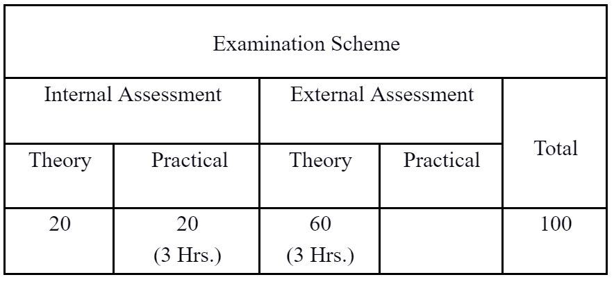
Evaluation
Text Books
- Floyd, “Digital Fundamentals”, PHI.
- Morris Mano. “Digital Design”, Prentice Hall of India.
- Tocci.R.J, “Digital systems-Principles & Applications”-Prentice Hall of India.
Reference Books
- B. R. Gupta and V.Singhal, “Digital Electronics” 4th Edition, S.K Kataria & sons, India.
- Flctcher.W.I., “An Engineering lrproach to Digital Design”, Prentice Hall of India.
- Millman & Halkias ,”Integrated ElectrOnics”.
- V.K.PUR1, “Digital Electronics”, TMH.,


No comments:
Post a Comment